

Advantest Unveils SiConic Test Engineering: Unified, Scalable Bench Environment for Debug and Validation
Extends SiConic Ecosystem to Empower Test Engineers Across Development Lifecycle—from Structural Test Bring-up to ATE and SLT Deployment
/EIN News/ -- TOKYO, May 08, 2025 (GLOBE NEWSWIRE) -- Leading semiconductor test equipment supplier Advantest Corporation (TSE: 6857) today unveiled SiConic Test Engineering (TE), the newest addition to the SiConic family introduced in February 2025. SiConic TE offers test engineers the ability to bring up and validate structural and functional tests over high-speed I/O (HSIO) interfaces in a scalable bench environment, enabling earlier validation and debug without occupying valuable ATE systems.
SiConic Link flexibly connects to standard evaluation boards through functional interfaces like USB, PCIe, control interfaces, and GPIOs. This is the foundation for SiConic TE to enable test engineers to rapidly validate and debug design verification (DV) and design for test (DFT) content in SiConic’s unified environment on the bench.
Building on the V93000 test system’s leadership in scan over USB or PCIe, SiConic’s unified environment brings native DV test content to test engineering without the error-prone and lengthy conversion and debug cycles typical for bring-up of advanced functional tests on ATE. Required for high-quality coverage in verification and test, functional testing enables a productivity boost for the bench collaboration of DV, DFT and test engineering. SiConic TE accelerates time-to-quality for both the V93000 and Advantest’s system-level test (SLT) and burn-in platforms with the ActivATE360™ suite of software tools.
Integrating seamlessly with SiConic Link hardware and the SmarTest 8 software platform, SiConic TE provides users with comprehensive access to functional HSIO links for enhanced throughput and rich trace capabilities during test execution. By enabling smoother handoffs between silicon validation (SV), DV and TE teams, SiConic TE fosters tighter cross-domain collaboration.
Through its unified test environment and shared ecosystem, SiConic TE improves the correlation between bench, ATE and SLT systems. The tool’s optimized engineering resources allow bring-up and debug to be offloaded from ATE to the bench, freeing up valuable tester capacity and enabling more effective scaling. In addition, tight integration with leading EDA partners enables cross-functional collaboration with DV and DFT teams, improving test content development and speeding first-silicon success.
“With SiConic Test Engineering, we’re expanding the SiConic vision to empower test engineers in a unified environment on the bench,” said Juergen Serrer, chief technology officer and executive vice president, SoC Test Business Unit, Advantest. “By moving bring-up and validation to scalable bench environments—and keeping DV, DFT, SV, and TE aligned through a scalable ecosystem—we’re helping customers validate faster, collaborate smarter, and maximize their engineering resources.”
According to G. Dan Hutcheson, vice chair, TechInsights, “Improving productivity at the R&D level is vital for design engineers. Advantest’s automated silicon validation approach would allow sign-off and test engineering to proceed concurrently using shared test data, helping ramp SoC designs more quickly, and shortening time-to-money, while ensuring design-to-system quality.”
Industry Support
Advantest developed SiConic TE in close collaboration with leading customers and EDA partners to ensure seamless integration into existing design and validation flows.
“Siemens EDA and Advantest have a long history of joint development on many DFT technologies, including Tessent Streaming Scan Network (SSN) and IJTAG,” stated Ankur Gupta, senior vice president and general manager, Digital Design Creation Platform, Siemens EDA, Siemens Digital Industries Software. “Collaborating on Advantest SiConic and Tessent In-System Test strengthens this long-running collaboration and helps to provide our users with time-to-market improvements and higher productivity.”
“As the scale and complexity of chips continue to increase, new verification approaches are needed to shift verification cycles earlier and deliver silicon with higher quality,” said Tom De Schutter, senior vice president of product management at Synopsys. “Our collaboration with Advantest enables users to develop drivers for high-speed interfaces, validate SERDES, and perform functional testing and structural testing through the combination of Advantest's SiConic platform and Synopsys’ HAPS-100 platform, VC Portable Stimulus, TestMAX SF/SEQ and SLM HSAT IP solutions.”
VOICE 2025
Attendees can learn more about the SiConic offerings during Advantest’s annual VOICE Developer Conference, May 12-14, 2025, in Austin, Texas.
About Advantest Corporation
Advantest (TSE: 6857) is the leading manufacturer of automatic test and measurement equipment used in the design and production of semiconductors for applications including 5G communications, the Internet of Things (IoT), autonomous vehicles, high-performance computing (HPC) including artificial intelligence (AI) and machine learning, and more. Its leading-edge systems and products are integrated into the most advanced semiconductor production lines in the world. The company also conducts R&D to address emerging testing challenges and applications; develops advanced test-interface solutions for wafer sort and final test; produces scanning electron microscopes essential to photomask manufacturing; and offers system-level test solutions and other test-related accessories. Founded in Tokyo in 1954, Advantest is a global company with facilities around the world and an international commitment to sustainable practices and social responsibility. More information is available at www.advantest.com.
ADVANTEST CORPORATION
3061 Zanker Road
San Jose, CA 95134, USA
Cassandra Koenig
cassandra.koenig@advantest.com
A photo accompanying this announcement is available at https://www.globenewswire.com/NewsRoom/AttachmentNg/14bf5d64-80f2-4c0c-8f9c-bc56928492f7

![]()
SiConic Test Engineering
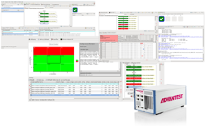
SiConic Test Engineering: A unified, scalable bench environment for debug and validation
Distribution channels: Conferences & Trade Fairs, Consumer Goods, Culture, Society & Lifestyle, Media, Advertising & PR ...
Legal Disclaimer:
EIN Presswire provides this news content "as is" without warranty of any kind. We do not accept any responsibility or liability for the accuracy, content, images, videos, licenses, completeness, legality, or reliability of the information contained in this article. If you have any complaints or copyright issues related to this article, kindly contact the author above.
Submit your press release